Research
I. Research Overview
My research focuses on the study of materials at the atomic scale to understand the fundamental phenomena of their formation and evolution. Understanding the fundamental phenomena of material formation and evolution is the key to make better quality materials for higher efficiency electronic devices. Specifically, I apply molecular dynamics (MD) simulations to study the growth and defect evolution of semiconductor materials for solar cell applications. MD simulations solve for the classical Newton’s Laws of Motion for a system of atoms using an interatomic potential. An interatomic potential contains information about the repulsion and attraction forces between two atoms separated by a distance.My research uses the Stillinger-Weber (SW) interatomic potential [1] to simulate the growth and evolution of Cadmium Telluride (CdTe) [2] which is a compound used for solar cell applications. CdTe is a good material for solar cells due to its ideal bandgap (~1.45 eV) and high absorption coefficient (>104cm-1). However, defects in the material at the atomic scale reduce its efficiency. Therefore, it is important to study this material at the atomic level to reduce its defects and make higher efficiency solar cells. In the next sections, I will summarize my research achievements and will discuss my future research directions.
II. Research Achievements
1) Enabling MD simulations of polycrystalline II-VI semiconductors
CdTe thin films for solar cells are usually fabricated using close space sublimation technique which results in highly defected polycrystalline films. Different treatments have been investigated to increase the quality of the polycrystalline CdTe growth. For example, Cadmium Chloride (CdCl2) has been used for decades as a post treatment to CdTe. The effect of the CdCl2 in the quality of the CdTe film is still not fully understood. However, studies have shown that the CdCl2 eliminates defects [3] and promotes grain growth [4]. Other treatments include rapid thermal processing [5], CdTe surface etching to obtain Te-rich surface [6], and Zinc Telluride (ZnTe) buffering [7]. Although these treatments have been successful to increase the quality of CdTe films, there is not a clear understanding about the growth of CdTe at the atomic scale.
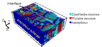
To address this problem, I proposed a method to model the growth of polycrystalline CdTe with no prior assumption of its grain and grain boundary type and evolution. To achieve this, I used MD simulations to grow an amorphous layer of CdTe material. Then, I used this amorphous layer as a substrate to grow polycrystalline material. The result was a “naturally grown” polycrystalline layer on top of the amorphous layer as seen in Figure 1 and which compares very closely to experimental polycrystalline films [8].
2) Explaining Cu clustering in CdTe
Cu in CdTe solar cells as a dopant and as back contact has been used for over 20 years. Studies show that the Cu replaces Cd atoms and forms CuxTe complexes which help the CdTe become a richer p-type layer [9]. Also, Cu forms a good ohmic contact with the CdTe by creating a smaller valence band offset [10]. Despite of the great benefits of using Cu, recent studies show that the copper is a fast diffuser and segregates into clusters over time. These clusters diffuse through grain boundaries to end up at the CdTe/CdS junction affecting the electronic properties of the junction and overall cell [11]. A question then arises about the origin of Cu cluster and how to control it.
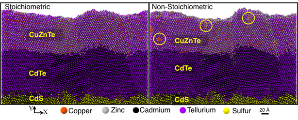
To address this problem, I proposed to develop an interatomic potential for CdTe that included Cu. An interatomic potential was successfully developed by our group in collaboration with Sandia National Laboratories. I used the potential to perform simulations of the incorporation of Cu in polycrystalline CdTe at various Cu loadings. The results showed that the Cu forms clusters only at non-stoichiometric compositions as seen in the yellow circles in Figure 2 where Cu has an excess over the other atoms. However, in the stoichiometric regime, the Cu incorporates mostly by forming CuxTe and does not form clusters [12]. Experimental results were performed by collaborators to validate our simulation results.
3) Quantifying the mobility of grain boundaries in CdTe
Recent studies debate about whether grain boundaries are beneficial or detrimental for solar cell performance. For example, highly symmetric grain boundaries such as S3 twin boundaries are not electrically active and therefore do not represent a thread for the performance of the solar cell [13]. On the other hand, high angle random grain boundaries such as high S coincide site lattices behave as recombination centers for carriers. Despite of the effort to understand the electronic behavior of grain boundaries, a better understating of grain boundary formation and evolution needs to be obtained. A generalization of the behavior of films at specific temperatures and pressures has been previously proposed, however the CdTe material is very complex containing wurtize and zincblende domains throughout the film.
To understand the evolution of the growth of polycrystalline CdTe better. I proposed to performed simulations on the motion of grain boundaries to quantify their mobility, and therefore discover the behavior of the CdTe film. The simulations consisted of a three dimensional simulation cell with periodic boundary conditions in all axis. Inside the simulation cell, there were two crystals of different orientations divided by a grain boundary parallel to the X-Z plane and located at the center of the simulation and at the end of the simulation cell. An energy V is applied to one of the grains and thus a force is created that makes the grain boundary move as to reduce the total energy of the system as seen in Figure 3. The simulations were applied to S3, S7, and S11 grain boundaries which are commonly seen in CdTe experimental results [14]. The results show that S3 grain boundaries have a high energy barrier compared to S7 and S11. This result agrees with the experimental observation that S3 grain boundaries are the most abundant grain boundary in CdTe [15].

III. Areas of Interest
My current research has many interesting possibilities in interdisciplinary research areas. Built upon the theoretical and experimental foundations I developed during my doctoral study, I plan to expand towards the study of other materials systems such as InxGa(1-x)N. Also, I plan to perform electronic calculations studies of the simulated polycrystalline growths. In the following, I outline the two main areas that I plan to develop in the future.
1) Growth simulation of InxGa(1-x)N to obtain cubic phase films
Indium Gallium Nitride (InxGa(1-x)N) is an excellent material for optical devices because it covers a wide spectral range from near infrared to ultraviolet. InxGa(1-x)N is suitable for laser diodes and electron mobility transistor for high-speed electronic devices. However, several challenges exist which prevent the InxGa(1-x)N alloys from being used effectively for solar cells. A major problem is the reduction in quantum efficiency at alloy compositions above x ~ 0.3 [16]. This problem is attributed to polarization of the alloy in the hexagonal phase. Therefore, an interest has recently emerged in cubic phase InGaN because there is a better dopant incorporation, no polarization due to its symmetry, and larger bandgap variation with respect to composition. However, technology to grow cubic phase InGaN material is still not existent. The proposed work is to perform a series of MD simulations at different temperatures and substrate polarizations to accomplish cubic phase growth.
2) Electronic DFT calculations of simulated polycrystalline CdTe
CdTe is an excellent material for solar cell applications due to its ideal bandgap and high absorption coefficient. However, the presence of material defects such as grain boundaries diminish the electronic properties of the material. Work has been done to study the electronic characteristics of grain boundaries computationally, however the structures used are artificially created as opposed to “naturally grown”. Most of the grain boundaries studied are planar bi-crystals based on 2-dimensional transmission electron microscope (TEM) images of low angle grain boundaries or created using algorithms [14], [17], [18]. The innovativeness of this research is that DFT calculations will be performed on grain boundaries within simulated polycrystalline structures that very closely resemble the texture of experimentally grown chalcogenides.
References
[1] F. H. Stillinger and T. A. Weber, “Computer simulation of local order in condensed phases of silicon,” Phys. Rev. B, vol. 31, no. 8, pp. 5262–5271, 1985.
[2] X. W. Zhou, D. K. Ward, J. E. Martin, F. B. Van Swol, J. L. Cruz-Campa, and D. Zubia, “Stillinger-Weber potential for the II-VI elements Zn-Cd-Hg-S-Se-Te,” Phys. Rev. B – Condens. Matter Mater. Phys., vol. 88, no. 8, pp. 1–14, 2013.
[3] T. Paulauskas et al., “Atomic-resolution characterization of the effects of CdCl2 treatment on poly-crystalline CdTe thin films,” Appl. Phys. Lett., vol. 105, no. 7, p. 071910, 2014.
[4] H. R. Moutinho, “Effects of CdCl[sub 2] treatment on the recrystallization and electro-optical properties of CdTe thin films,” J. Vac. Sci. Technol. A Vacuum, Surfaces, Film., vol. 16, no. 3, p. 1251, 1998.
[5] J. Li et al., “Controlled activation of ZnTe:Cu contacted CdTe solar cells using rapid thermal processing,” Sol. Energy Mater. Sol. Cells, vol. 133, pp. 208–215, 2015.
[6] F. R. Ahmad, J. R. Cournoyer, K. C. Raghavan, and B. a. Korevaar, “Tellurium-Rich CdTe, and the Effect of Tellurium Content on the Properties of CdTe,” J. Electron. Mater., vol. 43, no. 8, pp. 2888–2894, 2014.
[7] C. A. Wolden et al., “The roles of ZnTe buffer layers on CdTe solar cell performance,” Sol. Energy Mater. Sol. Cells, vol. 147, pp. 203–210, 2016.
[8] R. Aguirre, J. J. Chavez, X. Zhou, and D. Zubia, “High Fidelity Polycrystalline CdTe/CdS Heterostructures via Molecular Dynamics,” MRS Adv., vol. 2, no. 53, pp. 3225–3230, Jun. 2017.
[9] T. a. Gessert et al., “Pathways toward higher performance CdS/CdTe devices: Te exposure of CdTe surface before ZnTe:Cu/Ti contacting,” Thin Solid Films, vol. 535, pp. 237–240, 2013.
[10] D. Rioux, D. W. Niles, and H. Höchst, “ZnTe: A potential interlayer to form low resistance back contacts in CdS/CdTe solar cells,” J. Appl. Phys., vol. 73, no. 12, p. 8381, 1993.
[11] C. A. W. A. Abbas, D. M. Meysing, J. Li, J.D. Beach, T. M. Barnes, J.M. Walls, “Structural and Chemical Characterization of the Back Contact Region in High Efficiency CdTe Solar Cells,” 2015.
[12] R. Aguirre et al., “Crystal Growth and Atom Diffusion in (Cu)ZnTe/CdTe via Molecular Dynamics,” IEEE J. Photovoltaics, vol. 8, no. 2, pp. 594–599, 2018.
[13] M. M. Nowell, M. A. Scarpulla, N. R. Paudel, K. A. Wieland, A. D. Compaan, and X. Liu, “Characterization of Sputtered CdTe Thin Films with Electron Backscatter Diffraction and Correlation with Device Performance,” Microsc. Microanal., vol. 21, no. 04, pp. 927–935, 2015.
[14] J. Moseley et al., “Recombination by grain-boundary type in CdTe,” J. Appl. Phys., vol. 118, no. 2, 2015.
[15] R. Aguirre, S. Abdullah, X. Zhou, and D. Zubia, “Molecular Dynamics Calculations of Grain Boundary Mobility in CdTe,” Nanomaterials, vol. 9, no. 4, p. 552, 2019.
[16] J. Wu, “When group-III nitrides go infrared: New properties and perspectives,” J. Appl. Phys., vol. 106, no. 1, 2009.
[17] C. Li et al., “Grain-boundary-enhanced carrier collection in CdTe solar cells,” Phys. Rev. Lett., vol. 112, no. 15, pp. 1–5, 2014.
[18] Y. Yan et al., “Physics of grain boundaries in polycrystalline photovoltaic semiconductors,” J. Appl. Phys., vol. 117, no. 11, p. 112807, 2015.
